Low Noise Amplifier for 0.1Hz to 10Hz Measurements
Write-Up Contents
Revision History
- Initial breadboarding, May 2023
- Rev X1 design, testing, and modification
- Rev X2 design (abandoned)
- Rev X3 design and testing, July 2023
- Rev A design and testing, April 2024
- Rev B design and testing, July 2024

Rev A Enclosed LNA with Custom Gain and Frequency Response
Project Summary

Rev X3 enclosed LNA
This low noise amplifier (LNA) project was inspired by Marco Reps’ youtube video with ultra-precision LTZ1000 voltage references and his work on characterizing their noise. While I’m not quite a nanovolt-nut yet, I was going through initial design and prototyping of a modular SMU, and a low frequency LNA would be a valuable tool. Noise plots over the 0.1Hz to 10Hz range are a great way to characterize precision DC sources, and a suitable LNA allows these measurements to be made with a standard oscilloscope.
The main challenges designing such an LNA are to keep the amplifier’s noise floor low, and to build a stable 0.1Hz high pass filter. The capacitance required to achieve the noise goal is on the order of millifarads, which all but forces the use of electrolytic capacitors. Most designs I came across rely on hand-picking electrolytics with low leakage and waiting excessively for their leakage to settle, two things I was not willing to do.
After an initial breadboarding stage, I went through two PCB revisions to arrive at the current design. The overall gain is 5,000 V/V and the input noise floor is less than 11 nVrms and 91nVpp. The features I like most is the ~1 minute settling time and its insensitivity to electrolytic capacitor leakage. I achieved this by splitting the overall gain into two stages and adding a high pass filter between them. This setup only partially amplifies the DC offset due to electrolytic leakage, quickly discards it, then continues amplifying the signal of interest to the final gain.
LNA Specifications and Requirements
Low frequency LNA’s in this category have three main specifications: Noise floor, gain, and frequency response. Secondary features and specifications would include battery type, battery life, settling time, and protection features. Most design’s I’ve found have a gain of 10,000 V/V, a noise floor around 13nVrms / 100nVpp, a first-order 0.1Hz -3dB high-pass cutoff, and various orders of 10Hz high-pass cutoffs. Few I’ve seen offer any input protection, and the 9V battery life of Marco Reps’ design is under 1 hour.
Noise Floor
As far as noise specs, all values are “input referred” noise. Vpp is a nice value to know because it is a good measure of the worst-case deviation of a signal. However, noise calculations deal with Vrms values. There is no hard and fast rule linking the two, but through testing these LNA’s I’ve found that the Vpp measurement is typically 7x to 8x higher than the Vrms value. For the rest of the project write-up I’ll stick to mostly Vrms values. They are easier to follow for calculations, and are more consistent during testing.
Noise Calculations
For noise calculations, if a signal must pass through several series circuits, each with their own noise contribution. For such a system, if all noise sources are assumed to be random and gaussian, then calculating overall system noise of N individual noise sources follows the formula:
\(e_{overall} = \sqrt{e_{1}^2 + e_{2}^2 + … + e_{N}^2}\)
where each \(e_{x}\) is a Vrms value.
While knowing that formula is essential for calculating performance, the main takeaway is that for a system with a few noise sources, as soon as one source gets to be a couple times larger than the others it dominates the overall noise. A system with a 10.0nVrms noise source and a 1.0nVrms noise source has an overall noise of only 10.005nVrms. A system with a 10.0nVrms source and a 5.0nVrms source only has 11.2nVrms of overall noise. Understanding this formula allows for easy prioritization of noise reduction measures.
For this LNA there were two types of noise sources I entered into my calculations: opamps and resistors. Some opamps provide 0.1Hz to 10Hz plots or specs with Vpp values. Others provide noise density plots (which may or may not go down to 0.1Hz). If only a Vpp measurment was given, I divided it by a scalar factor of 7.5 to estimate the Vrms value. If a noise density plot is shown, and it was reasonably flat in the 0.1Hz to 10Hz frequency range, then the formula for Vrms is:
\(e_{n}=N_{0}\sqrt{f_{1}-f_{0}}\)
Where \(N_{0}\) is the noise spectral density value from the plot with units \(V/\sqrt{Hz}\), and \((f_{1}-f_{0})\) is (10Hz – 0.1Hz), which is the bandwidth of interest. If the noise density plot isn’t flat, then you hasve to estimate the integral of the noise desity vs the square root of frequency. Good approximations can be made by breaking the bandwidth of interest into several sections and estimating each section as flat, and combining their equivalent noises according as separate random uncorrelated sources.
The formula for resistor noise is:
\(e_{n}=\sqrt{4kTR(f_{1}-f_{0})}\)
Where k is the boltzmann constant and is equal to 1.38E-23, T is the temperature in Kelvin, R is the resistance in Ohms, and \((f_{1}-f_{0})\) is the bandwidth of interest in Hz.
In general, there are a few basic noise-reduction techniques.
Using lower value resistors, lower-noise semiconductors, limiting bandwidth, or paralleling multiple signal paths. When a signal goes through N parallel and identical stages, the noise contribution of that stage goes down by a factor of \(\sqrt{1/N}\). Since op-amps are often the dominant noise contributor in these LNA’s, its common to see multiple parallel amplifier circuits with their outputs summed resistively.
For systems with gain, it’s important to specify what the noise value is referenced to. For an LNA with a gain of 10,000, 13nVrms of noise at the input is much different than 13nVrms of noise on the amplified output! Input referred noise is the most common way of specifying noise, scaling the entire system’s noise to some equivalent value present at only the input of the system. Since all noise figures here are specified as input-referred, for the LNA analysis any noise source that comes after a gain stage must have its value divided by the gain of that stage before being used in any equations.
As an example, say a circuit has two series op-amp circuits. The first is a 3 V/V gain stage, and the second is just a buffer. If each stage has a 1µVrms input referred noise amplitude, the formula for the overall noise of the series combination would be:
\(e_{input} = \sqrt{1µV_{RMS}^2+(1µV_{RMS}/3)^2} = 1.054µV_{RMS}\)
It’s clear that noise sources after large gain stages have almost no effect on input referred noise, so much of the LNA noise optimization is aimed at reducing the input high pass filter and input amplifier noise figures.
Gain
The reason why these LNA’s need high gain is to bring the signal of interest well above the noise floor of the oscilloscope used to take the measurements. Ideally the noise floor of the oscilloscope would be several times smaller than the amplified noise floor of the LNA. So for an LNA with a 13nVrms noise floor and a gain of 10,000 V/V, the oscilloscope intrinsic noise should be at most 1/3 of the LNA output noise, which would be around 40µVrms.
Using a BNC shorting plug, I measured the input noise of my Rhode & Schwarz RTB2004 oscilloscope. To make the results relevant to this LNA, the overall capture time was set to 12 seconds and the 20MHz bandwidth limit was enabled. In the “sample” acquisition mode, the input noise was 80.5µVrms / 680µVpp. In the “Hi-res” mode, the input noise was 12.7µVrms / 115µVpp. The high-res mode averages several samples together, lowering noise and the effective sample rate / bandwidth. For my scope the the sample rate was 1.667MS/s in “sample” mode and 10.9KS/s in “Hi-res” mode. 10.9kS/s is plenty fast for the 0.1 to 10Hz signal of interest!
While increased LNA gain reduces the oscilloscopes noise contribution, it also limits the measurement range. I knew that for simplicity I’d like my LNA to run off a single 9V battery. That means my input range would be approximately 6Vpp divided by the overall gain (6V to allow for discharged batteries). Ideally the gain value would be allow a measurement range of down to the LNA noise floor and up to what the scope can measure directly.
Since my target noise floor was 35nVrms, and my scope’s intrinsic noise was only ~13µVrms, a gain of 2,000 V/V worked well. At the low end, the 35nVrms amplifier noise floor would amplify to 70µVrms, over 5x the scope’s noise. At the high end, the amplifier could accept inputs up to 3mVpp, which is over 20x what the scope can measure directly. A gain of 5,000 V/V is a better balance of both, but I didn’t use that value until the Rev X3 LNA.
Frequency Response

Other Features
The common designs use a single gain stage, placing huge importance on using an input capacitor with low leakage. Any input capacitor leakage current creates a DC voltage across the high pass resistor to GND, which then gets amplified by the full gain of the LNA. For the common 1kΩ resistor to GND and a gain of 10,000, it only takes 1µA of leakage current to create a 10V output offset, which is unacceptable. Unfortunately to keep the noise floor low, the input resistance can’t be much higher than 2kΩ, and therefore the input caps need to be at least 1mF to get the high pass cutoff down to 0.1Hz.
The amplification of the electrolytic leakage has another side effect: Long settling times. Electrolytic leakage is not constant with time, it changes every time its voltage changes. High
dialectric absorption
in electrolytics means it can take hours for the leakage to stabilize. Accurate noise measurements can’t be made until the leakage is nearly stable.
Another important aspect is input protection. I didn’t realize this for my X1 design, and didn’t add it until the X3 design. Say the input high-pass filter is a 1mF capacitor and a 1.6kΩ resistor, and the LNA is running off a fresh 9V battery for ±4.5V supply rails. A common test for this kind of LNA is measuring the noise on a precision 10V reference. When the reference is plugged in, the 1mF input capacitor is initially discharge. Suddenly the full 10V is presented to the input gain stage, which could easily overload and damage an opamp’s input. Inserting series resistance between the high-pass and opamps inputs is limited to only a couple hundred ohms to keep noise low. This may cause significant current to flow through the opamp clamping diodes, potentially damaging them, and potentially damaging the connected device.
While the 10V input case is somewhat manageable, high voltages like 20V or 30V, say from the output of a linear PSU or an SMU, can cause significant issues. At 30V, the input resistor will dissipate a peak of 0.56W, and will need to dissipate a total of 0.45 Joules to charge up the input cap. That’s enough to overload SMD resistors up to 0805, sometimes 1206. It also means that 30V will be dumped onto the opamp inputs, which is likely to cause damage.
I wanted to tackle all of these issues and design an LNA that could tolerate a reasonable range of electrolytic leakage, settle in a minute or two, and protect the input from voltages up to 30V.
New Topology and Theory of Operation
It was clear that the standard LNA topology would not meet my design requirements. The alternative I designed could take care the electrolytic leakage issues and provide fast settling with a straightforward change.

New LNA Topology
The main change was to split the overall gain into two stages and to add a high pass filter immediately after the first stage.
The main reason to make this split is to reduce the impact of the input electrolytic’s leakage and dielectric absorption. The first stage gain must be high enough to lift the input signal well above the noise floor of all the following stages. This can be accomplished with gain as low as 10 V/V if the following stages are fairly quiet. But going higher can also reduce the impact of other issues in the following stages. The gain also must not be so high that leakage currents create large DC offsets. The output of the first stage will have headroom limited by the supply rails, and that headroom will be used by any DC offset, plus 1/2 the peak to peak voltage of the input signal. If the following stages use active filtering, their limited input signal ranges must also be considered.
Immediately following the first stage is a high pass filter. This
completely removes the DC offset from the first stage and acts as the primary high pass filter. Since the signal is already amplified significantly, the noise of all the following circuits becomes negligible. This means getting the 0.1Hz cutoff frequency is much easier since resistors up to 1MΩ can be used with almost no noise impact. The higher allowable resistance means that the capacitors only need to be 1µF – 10µF, meaning small film or common SMD ceramic capacitors can be used. While the X7R and X5R ceramic capacitors in this range are a little microphonic and can translate thermal drift into changing voltages, any imperfections are directly divided by the first stage gain when referring them to the input. A sufficiently high first stage gain will make these issues negligible.
If the classic frequency response is to be maintained, the input high pass filter must have a cutoff significantly below 0.1Hz, since the primary high pass filter comes after the first stage gain. This isn’t difficult to achieve, since 2.2mF – 4.7mF electrolytic capacitors are reasonably sized and priced in the 25V – 50V range. Since this topology can tolerate significant leakage, finding a suitable input capacitor is relatively easy. Dielectric absorption and long settling times are not a concern, since the primary high-pass filter can use ceramic or film capacitors with next to no dielectric absorption, allowing settling time on the order of a couple minutes.
The second gain stage simply amplifies the signal to levels that are suitable for the oscilloscope. Again, noise levels aren’t critical. The overall gain of the LNA is a balance of oscilloscope noise contribution and output headroom, but in practice it’s easy to get good performance for both.
Rev X1 Design and Testing

X1 Topology
Input Stage
The input filter and gain stage of the LNA are the two largest contributors to the noise floor. Usually the input filter must be tuned to a precise 0.1Hz cutoff, but in my topology the input stage needed a lower cutoff. I chose a 2.2mF and 2kΩ input filter for its low noise and reasonable high impedance. The input cap is rated to 50V, since I’ve heard higher voltage electrolytics tend to have lower leakage, although I haven’t confirmed that. Even though the input resistor to ground is 2kΩ, the equivalent noise is only ~10nVrms since the input cap is essentially in parallel with the 2kΩ resistor, greatly lowering the impedance.
The dominant noise sources in my Rev X1 design are the 2kΩ protection resistor and the OPA2188 first stage opamps. I chose 2kΩ to limit the worst case input current to 20mA with a ~40V input, and its thermal noise is 18nVrms. Luckily the OPA2188 had a noise density vs frequency plot that went down to 0.1Hz, so I could calculate that its 0.1Hz to 10Hz rms noise is about 31.6nVrms. That was a little high, so I used two in parallel to bring the equivalent opamp noise down to 22.3nVrms. This makes the overall noise of the input stage:
\(\sqrt{22.3nVrms^2+18nVrms^2+10nVrms^2}=30nVrms\).
While it seems very close to my 33nV goal, that left plenty of headroom from my 33nVrms goal for the Rev X1 design. Since the noise of everything after the first stage is divided by 200, the allowable noise could go up to 2.7mVrms and I could still meet the 33nVrms input noise goal.
For input protection, I added back-to-back clamp diodes to GND. They are meant to protect the opamp’s inputs, but they don’t offer any significant protection for the input source. If a source was hot-plugged into the LNA, the input 2.2mF cap will initially appear as a short-circuit, and the two parallel input 2kΩ resistors are the only current limiters. There is also a case where the LNA was previously plugged into a higher voltage source, say 30V, and then connected to a new source that’s only 10V. In that case the input cap would dump current into the new source, again with only the two 2kΩ resistors to limit current. Overall this input protection scheme didn’t quite meet my initial goals, but at least protection of the LNA input was relatively assured.
Filtering Stages
Following the first stage gain is the main filter block. For this design I chose the overall frequency response to be a 3rd-order Bessel high pass filter at 0.1Hz, and a 5th order Bessel low pass filter at 10Hz. The choice of high pass filter is unusual, my logic was that a the LNA wasn’t meant to amplify frequencies lower than 0.1Hz, so a higher filter order would be better. Since I could use active filters in this topology, adding filter orders was simple. The filter is implemented with a a sallen-key active stage plus the output RC filter. Since noise wasn’t a concern anymore, 10µF ceramic capacitors were used, and the resistor values were 160k and 330k. The 10Hz low pass filtering on other LNA’s varies, but again I chose a high-order filter. The four filter poles are implemented in two sallen-key filters.
Output & Power Supply
The output is a simple 10x gain stage, followed by an RC high pass filter. This brings the overall gain to 2000 V/V, and removes any DC offsets from the LNA before being sent out of a BNC connector to the oscilloscope.
Testing
\(RMS_{AC} = \sqrt{RMS^2 – Mean^2}\)
The initial configuration of the X1 prototype achieved a 261nVpp and 36.3nVrms noise floor, very close to the initial goals.

Rev X1 shorted input noise floor
The next key test was to measure the frequency response. While my oscilloscope has a tracking generator and a Bode plotting function, its frequency range is software limited to 10Hz to 25MHz. Even if it could cover the low frequency range needed to test the LNA, going point-by-point through a whole frequency sweep would take a very long time.
I set up my HP 33120A signal generator to output a logarithmic frequency sweep from 50mHz to 20Hz over 200 seconds, and the envelope of the LNA output would be its frequency response. The oscilloscope horizontal cursors are set to the -3dB amplitude, and the vertical cursors are set to the points in time where the sweep was at 0.1Hz and 10Hz.
At first the high-pass cutoff was way off, it turned out to be some incorrect resistor values in the sallen-key circuit. I was fairly happy with the sweep method, but it still took 200 seconds, and the results had to be visually interpreted instead of automatically measured. Later I figured out a new frequency response measurement method that cut the capture time in half and provided a whole Bode-style amplitude plot.

Rev X1 frequency response
I had posted my initial results to metrology page of EEVBlog, and by now the comments and suggestions were rolling in. Unsurprisingly my decision to allow ceramic capacitors anywhere near my signal path raised quite a few questions. I started reworking and re-testing the LNA with a total of 16 different configurations.
The results were interesting, and I managed to lower the noise floor by 58% down to
13.2 nVrms and 102 nVpp. The biggest improvements came from reducing the input series resistance and by upgrading to a lower noise opamp. The original 2kΩ input resistor has similar noise levels to the two parallel OPA2188’s I used for the first stage gain, so reducing it to 100Ω resulted in a significant improvement. The OPA2188’s just happened to be the lowest noise opamps I had on hand, andswapping them for OPA2182’s reduced the noise further.

Rev X1 modifications and noise floor data
During this testing I also developed an input protection circuit. By passing the input signal through two series MOSFETs, one N-channel and one P-channel, and tying their gates to the positive and negative rails respectively, the voltage fed to the input amplifier stage was limited. For signals near zero volts, both MOSFETs would be turned on, and the signal would pass through. The MOSFETs don’t contribute much noise in this state because they are both fully saturated and their channel resistance is low.
When the input signal approaches the positive rail, at some point the Vgs of the N-channel mosfet gets too low, and it begins to turn off. The input voltage may still rise without being clamped, but the output voltage stops rising and will stay below the positive rail. The same thing happens with the P-channel MOSFET for negative signals. One added feature is that when the amplifier is switched off, neither MOSFET is turned on and no signal passes through, providing passive protection to the LNA even when off.

Rev X1 input protection modification

Rev X1 input protection clamped waveform
The input protection circuit was effective at limiting the voltage applied to the amplifier input, but that is not enough to protect most opamps. Since most opamps, including the OPA2188, have a pair of antiparallel diodes across their inputs, they would clamp and begin to draw current at very low voltages.

Rev X1 input current vs input voltage, OPA2188. Nonlinear and large current is due to the input clamp diodes conducting.
Texas Instruments has some opamps with what they call “MUX-friendly” inputs. Opamps with this feature do not have the input clamp diodes, and their inputs remain high-impedance for differential voltages up to the supply rail span. The OPA2182 has this feature, and has an extremely low noise floor. Swapping the input opamps for OPA2182’s resulted in a lower noise floor, and completely protected inputs.

Rev X1 input current vs input voltage, OPA2182. All current is due to input 2kΩ resistor to ground.
Settling time with this topology was excellent, about 30 seconds for small changes in input voltage, and about 2 minutes for the input capacitor leakage to drop low enough for the first stage to begin working. The current draw at 9V was 7.5mA total, giving a battery life of 80 hours.

Rev X1 input step settling time
Rev X2 and X3 Improvements
With all the X1 redlines figured out, I decided to order new revised board. I completed an X2 schematic and layout, but then decided I wanted to change the form factor, so I abandoned that revision and moved onto X3.
Rev X3 included the input protection circuit, OPA2182’s for the 1st stage, a gain of 5,000 V/V, an output for the first stage amplified signal, and a status LED. The first stage output allows for easy monitoring of the input leakage current, and can be used to observe larger signals that might otherwise be clipped by the higher gain main output. The status LED is lit when the output of the first stage is not railed, indicating that the LNA’s output is valid and almost settled.

Rev X3 LNA. I drilled the output BNC holes in the wrong spot, putting the battery on the wrong side!
The noise floor improved slightly, dropping to 90nVpp and 10.5nVrms Two of these LNA boards were purchased by EEVBlog users, and overall I’m happy with the electrical design.

Rev X3 vs X1 noise floor data
Rev A
Revision A includes an updated input protection circuit and some minor feature improvements. I discovered that the N-CH input protection MOSFET on the X3 LNA’s could be damaged by negative inputs -7V or below. Applying a negative voltage would quickly exceed its Vgs rating, causing both gate to source and drain to source to short out. To mitigate this a zener clamp circuit was added.

Rev A Enclosed Unit, Custom Gain and Frequency Response

Rev A Input Protection Circuit
The basic arrangement of Q3 and Q4 remains the same: Q3 blocks large positive input voltages, and Q3 blocks negative voltages. However, if a negative input is applied, the body diode of Q3 conducts, pulling its source down. In rev. X3 Q3’s gate was tied directly to VCC, and this scenario would break Q3. In rev. A, Q3’s gate is clamped to +10V max by D3. R36 pulls the gate up during normal operation and limits the current though D3 while it’s clamping. Those two components alone fully protect D3. However R36 is not enough to keep Q3’s gate voltage from rising above VCC during a positive input transient. Q3’s drain-to-gate capacitive coupling could push the gate above VCC, allowing the transient through. D4 is used to clamp the gate voltage to VCC, protecting the downstream amplifier.
Rev A also adds D2, a ±30V TVS diode. This clamps any ESD or applied transients, protecting Q3 and Q4. However if the LNA is misused, D2 could be damaged. During testing the large input capacitor is fully charged up to the input voltage. This can safely be as high as +30VDC. However, that voltage remains when the input is disconnected, the discharge time constant is approximately 40 minutes! If the input capacitor is left charged at +30V and a negative voltage is applied to the input, suddenly the negative terminal of the input capacitor falls to below -30V and D2 begins to clamp. Depending on the voltage swing and source impedance, this could damage D2 or the input source.

Rev A PCB with EMI Shield
Other new features include threaded panel-mount BNC connectors for simpler mounting, a new form factor to fit in a Hammond 1590Y enclosure, a negative input warning LED, wire points for simple switchable gain settings, and a metal EMI shield covering the input protection and first gain stage.

Rev A Panel Mount BNC Connectors
Of course no new board revision would be perfect, and I found a few items to rework. I realized that swapping the input for either output would easily damage the LNA. I decided to add some series resistors to each output, and some TVS diodes. For the main output I added a 2kΩ series resistor. There is already a DC blocking cap on this output, so the resistance just needs to limit the peak of any injected current. Other than that the DC blocking cap also protects the LNA. The x250 output is trickier to protect because it is DC coupled to the 1st stage output. I added a 4.99kΩ series resistor to limit the current. I needed a larger resistor to also limit power dissipation to 0.25W or less with ±30VD applied. That can be safely handled by a 1206 resistor, which was the largest part I had on hand that would fit. I also added a TVS diode to the power rails. Any current injected into the x250 output would bring up the power rails, and I wanted to clamp that to a safe value.

Rework on the Rev A Bottom Side

Rev A x250 Output Rework

Rev A Main Output Rework

Rev A Enclosed Unit Internal Layout
Other LNA's and Frequency Response Measurement
As I was testing the X3 design, Marco Reps posted a video about a low frequency LNA from Euler Precision. It was interesting to see their approach to achieving faster settling times and tolerance of input electrolytic leakage. They decided to use a single 10,000V/V gain stage, but used another circuit to trim the input and cancel any DC offset in the output. I admire the ingenuity, but I do think my two-stage topology is more practical and just as effective.
One aspect that interested me was their input filter. According to the label, it has a 1mF capacitor and a 1kΩ resistor for -3dB point of 0.159Hz. This confused me for a while, but I realized that choice of cutoff frequency results in an effective noise bandwidth of 0.101Hz, which makes sense for its application.
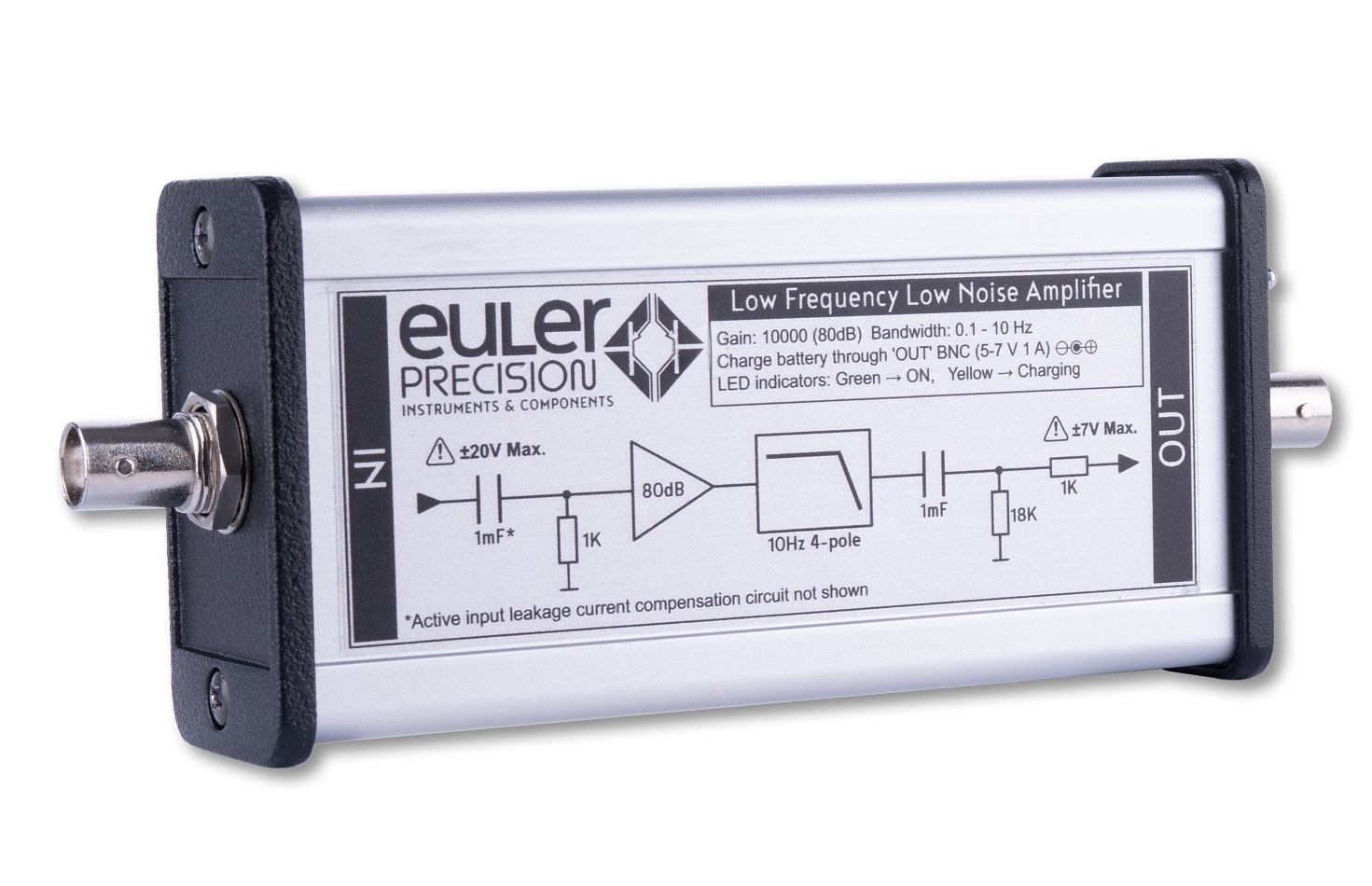
Euler Precision LFLNA-80 product image
Marco Reps did a teardown of the LNA, and that confirmed that the main input capacitor was 1mF, but that there was only a single 1mF 25V capacitor, and the stated input range is ±20V. There must be some input protection circuit to prevent reverse polarity across the input capacitor.

Euler Precision LFLNA-80 teardown image
Marco Reps also did a full frequency response analysis on this LNA, showing a -3dB point of 0.1Hz, so something isn’t lining up. My guess is the input resistor is actually larger than 1kΩ, and that their active offset cancellation circuit plays a role in setting the frequency response.

Euler Precision LFLNA-80 frequency response
I wonder how much the 3rd order high-pass filter on my LNA affects its measurements. I’ll have to perform more testing with it. Luckily I can easily turn the sallen-key high-pass stage into a simple buffered RC high-pass by only removing a couple parts.
One result of my LNA testing was the development of some python scrips for FFT based frequency response analysis. The sweeps I did with the signal generator were good enough for basic development, but are hard to pull precice values from. Full tracking generator sweeps like the one Marco Reps did take a very long time. The coarse analysis he did took over an hour.
The process of FFT based frequency response analysis is this: Feed a known function into the LNA, and use an oscilloscope to capture the response and save the plot data. Using python, the FFTs of both the input and output signals are calculated. The ratio of the FFT amplitudes is equal to the frequency response of the LNA, and a Bode plot is generated. The capture time has to be long enough to give good resolution at the lowest frequency of interest. Since each FFT bin separated linearly, and their spacing is set by the overall capture time, I had to perform 100 second captures to get good results in the 0.1Hz region.

FFTs of input step function and the X3 LNA output response

Calculated X3 LNA frequency response with -3dB reference line
I used a simple voltage step as my input, since it was easy to set up on the signal generator. Since the FFT of the input step is proportional to 1/f, the measured response also falls off at high frequency becomes dominated by noise not far past the 10Hz point. The noise present on the bode plot would probably raise concern about noise from the LNA, but its just an artifact of the measurement method.
I think this method is very interesting, since it captures the entire frequency response in one shot, with very usable results. While it is particularly well suited for low-frequency measurements, it may also be useful in cases where a tracking generator is not available, or cannot be connected. For example, the tracking generator on my oscilloscope is not floating, instead it is referenced to earth ground. This causes problems for analysis of power supply control loops, and I have to use an isolation transformer. A simple step signal may be easier to inject, and the input step doesn’t need to be synchronized or even measured by the oscilloscope for this method to work. Alternate input signals can also be used. I tried a sinc function with some success, it had good high frequency resolution with little noise, but the low frequency measurement was worse than the step function. Composite functions can also be used, and tuning the input waveform can help maximize the output signal to noise ratio.